Microstructure: The Missing Layer of Engineering
July 23, 2026In modern engineering, we have powerful tools for designing at two very different scales. At the smallest scale, computational chemistry gives us the ability to design molecules and crystal. . .
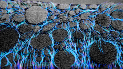
July 23, 2026In modern engineering, we have powerful tools for designing at two very different scales. At the smallest scale, computational chemistry gives us the ability to design molecules and crystal structures with remarkable precision. Researchers can now predict the behavior of proteins for pharmaceuticals, engineer catalysts for chemical reactions, and develop novel materials such as perovskites for next-generation solar cells. At the largest scale, engineers have been using sophisticated CAD software and continuum simulation tools for decades. These technologies make it possible to design and optimize complex systems ranging from aircraft wings and automotive chassis to bridges, turbines, bearings, and industrial machinery. Geometry, stress distributions, fluid flow, and thermal behavior can all be modeled before a physical prototype is ever built. The gap between atoms and systemsHowever, between these two scales sits something just as important, but historically far less understood: microstructure. Microstructure refers to the internal architecture of materials at the microscale, typically ranging from tens of nanometers to hundreds of microns. It encompasses the arrangement of grains and phases, particles and pores, interfaces and defects that emerge during manufacturing. Unlike molecules or engineered components, microstructure is rarely specified directly. Instead, it develops as a consequence of processing conditions such as temperatures and pressures, cooling rates, mixing speeds, deposition parameters, and heat treatments. This creates a fundamental challenge. Engineers ultimately care about performance: how strong a material is, how quickly a battery charges, how efficiently a catalyst work, or how reliably a pharmaceutical tablet dissolves. Yet the only variables they can directly control are the process parameters. The highly nonlinear relationship between process and performance is mediated by microstructure, making design an indirect and complex problem. And yet, microstructure exerts an enormous influence on the performance of many of the most important materials in the world. In pharmaceuticals, the connectivity of pore networks governs dissolution rates and drug delivery behavior. In battery electrodes, subtle changes to particle arrangement and porosity can dramatically influence ion transport, reducing charging times and improving energy density. The same alloy composition can produce steels with order-of-magnitude differences in strength and toughness depending on how processing affects grain size and phase distribution. In catalysts, activity can increase by factors of more than one hundred simply through changes in accessible surface area and pore morphology. Microstructure also plays a critical role in semiconductors, fuel cells, composites, filtration membranes, ceramics, and additive manufacturing. Across industries, the ability to control microstructure often determines whether a material remains a laboratory curiosity or becomes a commercially viable product. Unlike molecules or engineered components, microstructure is rarely specified directly. Instead, it develops as a consequence of processing conditions such as temperatures and pressures, cooling rates, mixing speeds, deposition parameters, and heat treatments. (Polaron)The least digitized layer of engineeringDespite its importance, microstructure remains one of the least digitized aspects of engineering. Today, most materials engineers are navigating this design space using intuition they’ve developed through years of experience and sparse experimental data. The workflows used to study microstructure are fragmented across many specialized tools. Imaging, segmentation, reconstruction, simulation, statistical analysis, and optimization are typically performed in separate software environments, often requiring significant manual effort to connect them together. As a result, systematic exploration of microstructural design spaces is slow and expensive to reproduce. Valuable data is frequently trapped in disconnected workflows, making it challenging to extract insights at scale. At the same time, the amount of data available to study microstructure is growing exponentially. There are now well over 100,000 scanning electron microscopes installed around the world, generating enormous volumes of image data every day. Additional imaging technologies, such as X-ray tomography and optical microscopy, are producing even larger datasets. Despite this abundance of information, most of the data remains underutilized. Images are often used for visual inspection, archived, and never fully analyzed. Discovery is only the startThis represents one of the largest untapped opportunities in materials science. There are many exciting AI companies working to accelerate materials discovery by identifying new chemistries and compositions. These efforts are important and have the potential to unlock entirely new classes of materials. But discovery alone is not enough. Microstructure encompasses the arrangement of grains and phases, particles and pores, interfaces and defects that emerge during manufacturing. (Polaron)When a promising material is found, its microstructure still needs to be engineered before it can meet the requirements of real-world applications. Performance, manufacturability, reliability, and cost are all heavily influenced by microstructural design. In many cases, the difference between a successful product and a failed one lies not in the chemistry itself, but in how the material is processed and how its microstructure evolves. That is why microstructure will sit at the heart of some of the most important technologies of the 21st century. The fundamental challenge is that microstructure is inherently stochastic. Unlike atoms, which follow well-defined interaction rules, or engineered components, which have explicitly designed geometries, microstructures are statistical systems. No two regions of a material are identical. Their complexity arises from countless interacting physical processes that occur during manufacturing. As a result, microstructures cannot easily be captured using simple analytical equations or represented by a conventional engineering drawing. Traditional modeling approaches often require significant simplifications that fail to capture the richness of real materials. But that same complexity makes microstructure perfectly suited to data-driven approaches. Designing microstructure with AIRecent advances in machine learning, computer vision, and generative modeling now allow us to learn the statistical structure of materials directly from microscopy data. Rather than relying solely on simplified physics-based representations, we can build models that capture the full distribution of realistic microstructures observed in experiments. These models enable entirely new capabilities. They can reconstruct three-dimensional structures from a single two-dimensional image, generate realistic synthetic microstructures, quantify uncertainty, explore vast design spaces, and uncover relationships between processing conditions and material performance. They provide a framework for understanding materials not as isolated images, but as statistical systems that can be analyzed, simulated, and ultimately, designed. At Polaron, we are building the AI infrastructure that makes this possible. Our platform brings together microstructure characterization, generation, simulation, and optimization into a unified workflow. By integrating these capabilities into a single environment, we enable researchers and engineers to move seamlessly from raw microscopy data to actionable design insights. Instead of navigating fragmented toolchains, teams can systematically explore microstructural design spaces and make data-driven decisions with greater speed and confidence. The implications extend far beyond improving existing workflows. Laboratories are becoming increasingly automated. Robotic experimentation platforms are accelerating the pace of materials development. High-throughput synthesis and characterization systems are generating more data than ever before. As these technologies mature, the ability to rapidly characterize, model, and reason about microstructure will become a critical capability. Without it, microstructural analysis risks becoming the bottleneck in automated materials discovery and development. For decades, microstructure has been the missing layer of engineering: too complex for traditional modeling approaches, yet too important to ignore. Samuel Cooper is chief scientist at Polaron. (Polaron)Today, advances in AI, machine learning, and generative modeling are finally providing the tools needed to understand and design this hidden layer of materials. The atomistic models tell us what is possible. The device-level models tell us what is required. But it’s the microstructure that decides what actually happens. And with AI, that missing layer is finally becoming something we can see, design, and control. Samuel Cooper is a professor at Imperial College London and chief scientist at Polaron. He wrote this article for SAE Media. More From SAE Media Group